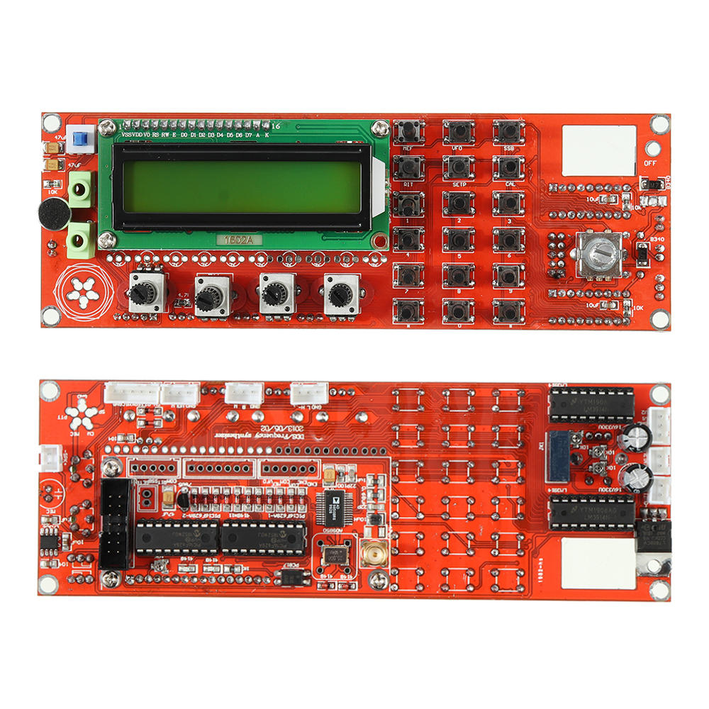
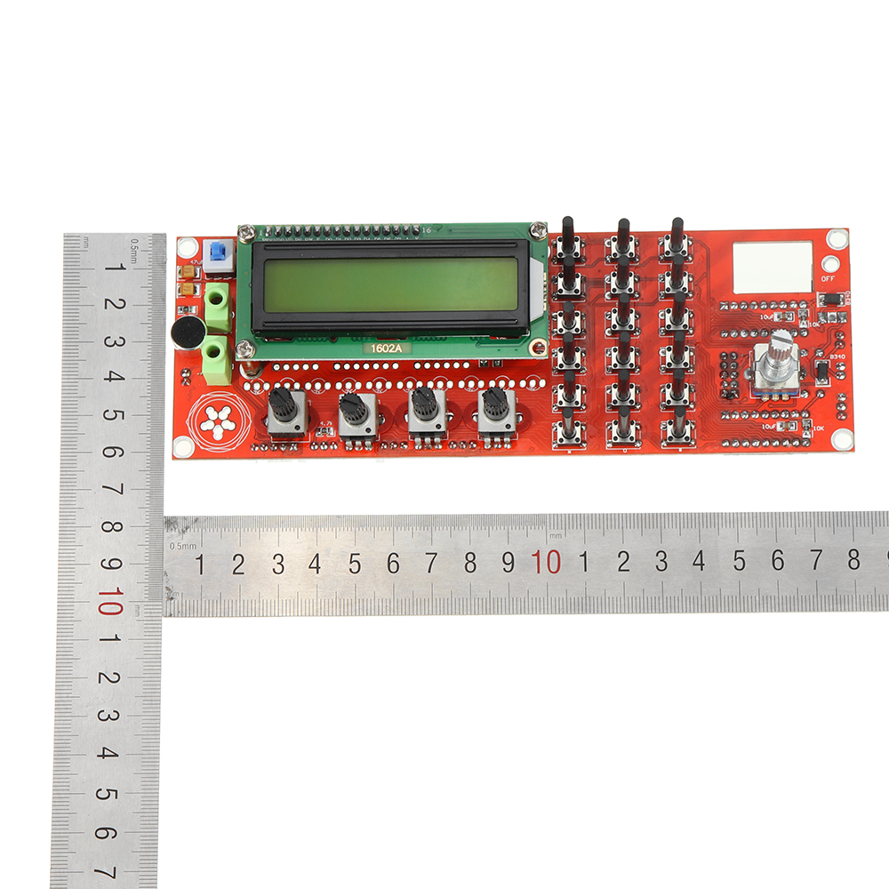
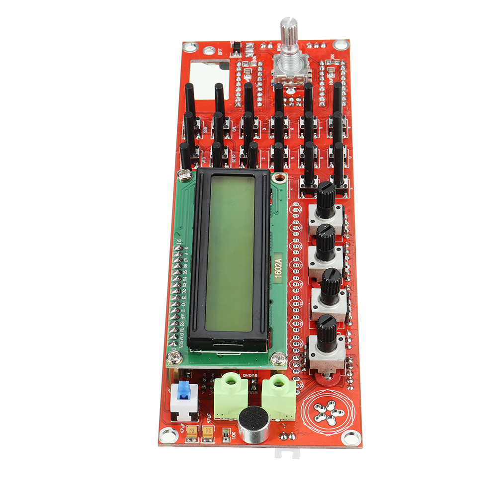
0-55MHz AD9850 DDS Signal Generator Shortwave Radio Wave Band Module for HAM Radio SSB6.1 Transceiver VFO SSB

Introduction:
This is a finished product, DDS, digital direct input frequency, with the volume potentiometer potentiometer, amplifier gain bandwidth potentiometer, AGC potentiometer, S - LED table display, a standing wave - LED table display
Feature:
12V input
12V output
Standing wave power into the detection signal.
Common ground
Manual gain control
Bandwidth power regulation, altogether
The corresponding motherboard microphones horn PPT and the CW
The mainboard control mode and band
DDS test power supply, no need welding
Use debug settings
The external button wiring methods:
In Fig KB-2 and KB-1 is an external key interface, which is the first leg leftmost respective interface common pin, which were co-phase four feet, their respective functions, such as KB-1: 1 -2 connected to complete work mode control switching functions, such as KB-1: 1-4 is connected to enable adjustment of stepping.
ENC image above coding switch feet, which, under the view of the switch of A contact pin 2 KB-2, and the drawing of B then KB-2 Pin 3, the drawing of C continued on the KB-2 1 foot.
Work mode and band control function:
Due to the limited capacity of the microcontroller itself, drive, or external relay operating voltage is different, not directly drive a relay, drivers need to work mode and operating band needs an external drive circuit, a specific circuit can refer to other materials.
LCD backlight connection:
Taking into account the number of people may use their own configuration LCD display, LED backlight may be because of different polarity, so the PCB, the 15 and 16 feet are vacant, and ask all of you to connect the LCD according to the polarity used.
It provides the LCD backlight connection, 16 feet grounded, 15 feet in series a 51 ohm resistor connected to + 5V power supply is like, if you want to keep off the backlight, you can take a switch to + 5V control.
DDS debugging:
The DDS control chip PIC16F628A-1 and PIC16F628A-2 has written VER4.06 program, after all the installation is complete, the access 5V supply, the 10K potentiometer to adjust the contrast, you can see on the screen under normal circumstances character, if not normal, measure the operating voltage of the microcontroller and display section. The set voltage polarity protection, so it will not happen to burn case you die.
If the LCD can not display the characters, please try to exchange PIC16F628A, because the two programs are different chips, follow my number marked on the component installation.
DDS key instructions and steps:
1. One key interface description:
ENC coding switch wiring feet
MEM storage mode conversion
VFO VFO A converted to VFO B, or by a VFO B switch to VFO A.
Conversion SSB operating mode, USB LSB AM CW cycle conversion.
RIT fine-tune the reception frequency.
STEP adjustment buttons.
CAL function setting button.
2. Wherein the KB-1 and KB-2 has a common pin, but not ground, please pay attention when installing.
3. Hold down the CAL button, power boot into the initial settings interface, and release the CAL button.
A: ENABLE 6XREFCLE: Set chip clock mode, adjust the frequency encoding switch settings, AD9851 set to 6 octave, AD9850 set to 1 octave, press CAL to enter the next item.
B: DDS-SYSTEM-CLK: the chip operating frequency is set, adjust coding switch to change the value, with the STEP key adjustment step, AD9851 set to 6 multiplier value of active Zhong, AD9850 set to the actual output of the source Restructure value, press CAL to enter the next item.
C: MIN_RX_DDS_FREQ: minimum operating frequency setting, adjust encoding switch to change the value, with the STEP key adjustment step should be set larger than the intermediate frequency value, press CAL to enter the next item.
D: MAX_RX_DDS_FREQ: maximum operating frequency setting, adjust encoding switch to change the value, with the STEP key adjustment step, should be set to 60MHZ or less can be, short press CAL to enter the next item.
E: SSB_OFFSET: SSB mode trim, adjust coding switch to change the value, with the STEP key adjustment step, press CAL to enter the next item.
F: CW_OFFSET: CW operating mode to fine-tune and adjust coding switch to change the value, with the STEP key adjustment step, press CAL to enter the next item.
G: OFFSET_FREQ: MF setting, as set 9MHZ or 10.7MHZ, adjust encoding switch to change the value, with the STEP key adjustment step, press CAL to enter the next item.
H: MULTIPLIER: multiplier setting should be set to 1, press CAL to enter the next item.
I: The display prompts SAVE, automatically save the contents of the above temples and return to normal operation.
Notes:
1. DDS SYSTEM CLK can be measured by the frequency after 30MHZ active crystal, the measured value is multiplied by 6, the calculated value is set here, if you are using AD9851, initially set to 180 million on the line.
2. OFFSET FREQ intermediate frequency settings can be set to + or -, rotary switch to change the value, hold down the STEP key, then coded rotary switches to adjust the step. In addition the value of the minimum operating frequency plus the intermediate frequency must be greater than zero.
Package includes:
1 x Signal Generator


0-55MHz AD9850 DDS Signal Generator Shortwave Radio Wave Band Module for HAM Radio SSB6.1 Transceiver VFO SSB See detail

